• chevron_right

      TSMC’s $65 billion bet still leaves US missing piece of chip puzzle

      news.movim.eu / ArsTechnica · 7 days ago - 13:38

    President Biden speaking at the official opening of TSMC’s first Arizona fabrication plant in December 2022. The Taiwanese chipmaker plans to start manufacturing 2-nanometer chips in the US in 2028.

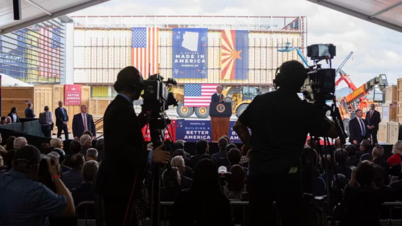
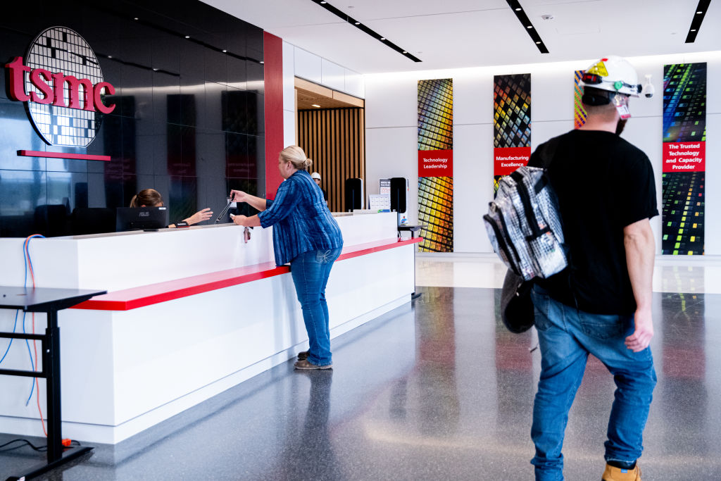
    Enlarge / President Biden speaking at the official opening of TSMC’s first Arizona fabrication plant in December 2022. The Taiwanese chipmaker plans to start manufacturing 2-nanometer chips in the US in 2028. (credit: Caitlin O’Hara/Bloomberg via Getty)

    Taiwan Semiconductor Manufacturing Company’s decision to bring its latest technology to America is a big step forward for US President Joe Biden’s quest for security in the vital tech supply chain—but still leaves Washington short of being able to completely produce the most complex chips in the US.

    The world’s biggest chipmaker by sales must also pull off an intricate balancing act as it steps up its US presence, satisfying customers such as Nvidia without damaging its highly profitable business model, which has underpinned the development of the global semiconductor industry for more than 30 years.

    TSMC’s planned $65 billion of investments in Arizona are part of a construction race in the US that involves other global chipmakers such as Samsung and Intel, which are also taking big subsidies from Washington.

    Read 30 remaining paragraphs | Comments

    • chevron_right

      TSMC will build third Arizona fab after winning $6.6B in CHIPS funding

      news.movim.eu / ArsTechnica · Monday, 8 April - 15:37

    The TSMC facility in Phoenix, Arizona.

    Enlarge / The TSMC facility in Phoenix, Arizona. (credit: The Washington Post / Contributor | The Washington Post )

    The US Department of Commerce has proposed another round of CHIPS Act funding up to $6.6 billion for Taiwan Semiconductor Manufacturing Company (TSMC), which President Joe Biden hopes will "support the construction of leading-edge semiconductor manufacturing facilities right here in the United States."

    With this award—which includes additional funding up to $5 billion in low-cost government loans—TSMC has agreed to increase funding in Arizona fabrication plants to $65 billion. That's the largest foreign direct investment in a new project in US history, the Commerce Department said, and it will fuel construction of TSMC's third Arizona fab.

    According to Biden, "these facilities will manufacture the most advanced chips in the world," putting the US "on track to produce 20 percent of the world’s leading-edge semiconductors by 2030."

    Read 13 remaining paragraphs | Comments

    • chevron_right

      Le séisme à Taïwan a aussi fait trembler l’industrie tech

      news.movim.eu / Numerama · Wednesday, 3 April - 16:07

    taiwan séisme

    Il s'agit de l'une des entreprises les plus en pointe dans le monde pour ce qui est de la production de semi-conducteurs. TSMC a toutefois été aussi confrontée au tremblement de terre qui a secoué Taïwan. Une secousse qui a aussi fait trembler l'industrie de la tech.

    • chevron_right

      TSMC “still assessing” chipmaking facilities after 7.4-magnitude quake hits Taiwan

      news.movim.eu / ArsTechnica · Wednesday, 3 April - 16:06

    TSMC's headquarters, seen here, are in Hsinchu, Taiwan.

    Enlarge / TSMC's headquarters, seen here, are in Hsinchu, Taiwan. (credit: Sam Yeh via Getty Images )

    Chipmaking operations at Taiwan Semiconductor Manufacturing Co. (TSMC) were briefly paused today following a 7.4-magnitude earthquake hit Taiwan, according to a company statement provided to Bloomberg and others .

    TSMC says that workers were evacuated as part of its earthquake safety protocols and that they have already returned to work. Bloomberg reports that the company is still "examining impact" to its operations, but it "expects to resume production overnight."

    The quake's epicenter was on Taiwain's east coast and has prompted tsunami warnings in Japan, China, and the Philippines, according to The New York Times . The quake was followed by a long series of over 200 aftershocks, including one 6.5-magnitude aftershock. It's the strongest earthquake to affect Taiwan since the 7.7-magnitude Jiji earthquake in 1999. As of this writing, the NYT reports that at least nine people have died and 1,011 have reported injuries.

    Read 4 remaining paragraphs | Comments

    • chevron_right

      US funds $5B chip effort after lagging on semiconductor innovation

      news.movim.eu / ArsTechnica · Friday, 9 February - 17:35

    US President Joe Biden speaks before signing the CHIPS and Science Act of 2022.

    Enlarge / US President Joe Biden speaks before signing the CHIPS and Science Act of 2022. (credit: Chip Somodevilla / Staff | Getty Images North America )

    The Biden administration announced investments Friday totaling more than $5 billion in semiconductor research and development intended to re-establish the US as a global leader manufacturing the "next generation of semiconductor technologies."

    Through sizeable investments, the US will "advance US leadership in semiconductor R&D, cut down on the time and cost of commercializing new technologies, bolster US national security, and connect and support workers in securing good semiconductor jobs," a White House press release said.

    Currently, the US produces "less than 10 percent" of the global chips supply and "none of the most advanced chips," the White House said. But investing in programs like the National Semiconductor Technology Center (NSTC)—considered the "centerpiece" of the CHIPS and Science Act's four R&D programs—and training a talented workforce could significantly increase US production of semiconductors that the Biden administration described as the "backbone of the modern economy."

    Read 11 remaining paragraphs | Comments

    • chevron_right

      The race between Intel, Samsung, and TSMC to ship the first 2nm chip

      news.movim.eu / ArsTechnica · Monday, 11 December - 15:15

    Abstract picture of a chip

    Enlarge (credit: zf L via Getty )

    The world’s leading semiconductor companies are racing to make so-called “2 nanometer” processor chips that will power the next generation of smartphones, data centers and artificial intelligence.

    Taiwan Semiconductor Manufacturing Company remains the analysts’ favorite to maintain its global supremacy in the sector, but Samsung Electronics and Intel have identified the industry’s next leap forward as a chance to close the gap.

    For decades, chipmakers have sought to make ever more compact products. The smaller the transistors on a chip, the lower the energy consumption and the higher their speed. Today, terms such as “2 nanometer” and “3 nanometer” are widely used as shorthand for each new generation of chip, rather than a semiconductor’s actual physical dimensions.

    Read 26 remaining paragraphs | Comments

    • chevron_right

      New chip-packaging facility could save TSMC’s Arizona fab from “paperweight” status

      news.movim.eu / ArsTechnica · Thursday, 30 November - 19:25 · 1 minute

    Apple wants to build more of its A- and M-series chips in the United States.

    Enlarge / Apple wants to build more of its A- and M-series chips in the United States. (credit: Apple)

    Late last year, Apple CEO Tim Cook announced that the company would definitely be buying chips made at Taiwan Semiconductor's new Arizona-based fab once it had opened. Apple working with TSMC isn't new; most, if not all, of the processors currently sold in Apple's products are made on one of TSMC's many manufacturing nodes. But being able to buy them from a US-based facility would be a first.

    The issue, as outlined by some TSMC employees speaking to The Information in September , is that the Arizona facility would manufacture chips, but it wouldn't be building a facility to handle packaging. And without packaging, the Arizona factory would essentially be a "paperweight," requiring any chips made there to be shipped to Taiwan for assembly before they could be put in any products.

    Today Apple announced that it had solved that particular problem, partnering with a company called Amkor to handle chip packaging in Arizona. Amkor says that it will invest $2 billion to build the facility, which will "employ approximately 2,000 people" and "is targeted to be ready for production within the next two to three years." Apple says that it has already worked with Amkor on chip packaging for "more than a decade."

    Read 5 remaining paragraphs | Comments

    • chevron_right

      TSMC, Samsung seeking permanent US licenses to operate China chip plants

      news.movim.eu / ArsTechnica · Friday, 13 October, 2023 - 18:43

    Aerial photo taken at night shows the TSMC plant area in Nanjing, Jiangsu province.

    Enlarge / Aerial photo taken at night shows the TSMC plant area in Nanjing, Jiangsu province. (credit: NurPhoto / Contributor | NurPhoto )

    The US Commerce Department announced today that key foreign chipmakers can continue receiving critical US chipmaking tools at China-based plants, Reuters reported .

    This decision extends special authorizations that were granted to foreign chipmakers—including South Korea's SK Hynix and Samsung, as well as the Taiwan Semiconductor Manufacturing Co (TSMC)—after the Biden administration curbed shipments of advanced chips and chipmaking equipment to China last October.

    Those export controls were intended to slow down China's rapid advancement of AI and military technologies, but the new rules also ended up negatively impacting US chip production. To overcome those inadvertent impacts on US chip supplies, the Biden administration granted limited special authorizations to allow some chipmakers to continue shipping equipment into China. Now, those chipmakers will be able to continue operating Chinese plants "without the headache of applying for US licenses," Reuters reported.

    Read 15 remaining paragraphs | Comments

    • chevron_right

      A17 Pro de l’iPhone 15 Pro : la première puce 3 nm est pleine de promesses

      news.movim.eu / Numerama · Wednesday, 13 September, 2023 - 06:30

    La très attendue première puce de l’histoire gravée en 3 nm apporte des améliorations technologiques sur tous les éléments internes (CPU, GPU, NPU). Loin de promettre une autonomie encore plus importante à un terminal déjà très endurant, elle est surtout utilisée pour faciliter l'ajout de fonctions (ray-tracing) et d'éléments (capteurs d’images plus grands) énergivores. [Lire la suite]

    Abonnez-vous aux newsletters Numerama pour recevoir l’essentiel de l’actualité https://www.numerama.com/newsletter/